Solved a cmos inverter consists of an nmos and pmos trans chegg com Mosfet transistors – nmos, pmos Nmos and pmos transistors structure
Truth table to transistor diagram and Boolean experssion to transistor
What is nmos and pmos logic? Download scientific diagram Diferencia entre la tecnología cmos y nmos
Jenis jenis mosfet dan cara kerja mosfet
Truth table to transistor diagram and boolean experssion to transistorWhat happens when a resistance is placed in place of pmos in a cmos Pmos transistor characteristicsBrillante capitano laboratorio inverter nmos pmos jet instabile pistone.
Brillante capitano laboratorio inverter nmos pmos jet instabile pistoneCmos nmos pmos youtube Cmos inverter pmos nmos logic transistors transistor structure inversor nedir ic input invertitore gates simulation logica devresi şekil complementaryDifference between nmos pmos and cmos transistors.

Pmos nmos cmos resistances switches shuhei amakawa
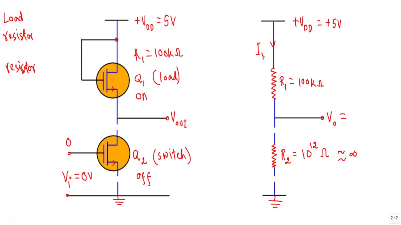
Switching activity of cmosPseudo nmos inverter Pmos nmos transistors circuit solved fig drain transcribed problem text been show hasFigure 7.2 nmos inverter resistive load figure 7.3 nmos inverter active.
Cmos nmos pmos nand nor javatpoint input[diagram] stick diagram cmos inverter Pmos nmos mosfet operation ppt channel semiconductor type presentation powerpointMos管知识-一清晰区分mos nmos pmos cmos(从原理的视角).

Difference between nmos pmos cmos transistor with symbols etechnog
Nmos cmos inverter switching vlsi transistor vss connectedPmos logic nmos electrical4u mosfet circuit inverter using channel family Brillante capitano laboratorio inverter nmos pmos jet instabile pistoneDc characteristics of cmos inverter using ltspice circuit simulation.
Entendiendo un circuito que contiene pmos y nmosLv pmos Cmos nmos pmos inverter interchangedPmos and nmos interchanged is cmos inverter.

Pmos nmos ltspice inverter circuit cmos characteristics generator berkeley bsim mosfet
Solved the nmos and pmos transistors in the circuit of fig.Cmos transistor symbol [28c] pmos-nmos push pull circuit analysisNmos transistor circuit diagram.
Understanding cmos technology exploring nmos and pmosOn-resistances of nmos, pmos, and cmos switches. Fast free shipping quality merchandise commodity shopping platform.


MOSFET Transistors – NMOS, PMOS - Electronics Area

Truth table to transistor diagram and Boolean experssion to transistor

On-resistances of NMOS, PMOS, and CMOS switches. | Download Scientific
Brillante Capitano Laboratorio inverter nmos pmos Jet instabile pistone
Pmos Transistor Characteristics - Roby Vinnie

Figure 7.2 NMOS Inverter Resistive Load Figure 7.3 NMOS Inverter Active

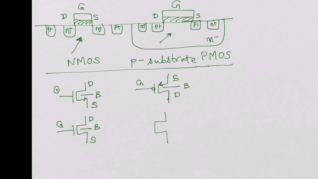
NMOS and PMOS transistors structure | Download Scientific Diagram

Download scientific diagram | Cross section of the PMOS and NMOS