Jfet circuit diagram » wiring draw and schematic Explain the structure and working of jfet. : electric guider The basic circuit of the source-coupled jfet oscillator.
jfet circuit diagram - Wiring Diagram and Schematics
Jfet circuit diagram Jfet schematic channel symbols field effect junction symbol transistor electronics circuit basics electrical drain choose board source construction Jfet-junction field effect transistor
2n3819 n-channel jfet pinout, datasheet, example circuit, features
Output characteristics of jfet circuitExplain the structure and working of jfet. : electric guider Jfet circuit diagramJfet biasing method bias voltage divider biased.
Jfet_vfo12) jfet circuit diagram and its characteristics Jfet construction working biasing transistor gate junction effect field current sourav gupta janCircuit diagram of n channel jfet.

N channel jfet circuit diagram
How to build an n-channel jfet switch circuitField-effect transistor (fet). junction field-effect transistor (jfet Jfet switch circuit channel diagram build schematic2n5457 n-channel jfet : datasheet, working & its applications.
Junction field-effect transistors (jfet) selection guide: typesJfet transistor symbols schematic effect field junction channel Single_ended_jfetJfet circuit diagram.

Jfet construction working bjt between explain difference fig ii two
[diagram] circuit diagram of jfetJfet circuit diagram 2n5457 n-channel jfet pinout, examples, features and datasheetJfet oscillator coupled.
Jfet circuit diagramJfet switch pinout datasheet example Jfet-junction field effect transistor,construction,symbol,operationWhat is jfet: its construction, working and biasing.
![[DIAGRAM] Circuit Diagram Of Jfet - MYDIAGRAM.ONLINE](https://i2.wp.com/www.researchgate.net/profile/Serges_Zambou/publication/311453582/figure/download/fig6/AS:436435359670278@1481065706472/Schematic-of-an-n-channel-Junction-Field-Effect-Transistor-JFET-with-the-three.png)
Jfet operation transistor characteristics
Jfet circuit diagramCircuit diagram of jfet Jfet vfo circuit diagram oscillator seekic processing signal simplePinout jfet datasheet transistor drain gate.
Jfet transistor polarity conventions effect field junction construction circuit operation symbol electronicsJfet n-channel and p-channel schematic symbols Amplifier jfet common source gain input circuit fet voltage signal small transistor amp given schematic formula type bjt emitter electronicsJfet circuit diagram ended single amplifier seekic basic ic transconductance.

Jfet explain majority
Transistor jfet effect field junction ppt fet onlineJfet mosfet fet effect field junction vs diagram comparison transistor channel circuitstoday basic symbol transistors bjt gif schematic information credit Common source jfet amplifier with ac equivalent circuitJfet: junction field effect transistor construction and working.
Jfet transistor junction construction byjusJfet biasing method Jfet characteristics circuit outputJfet transistor: operation and characteristics.

Explain the construction and working of a jfet . what is the difference
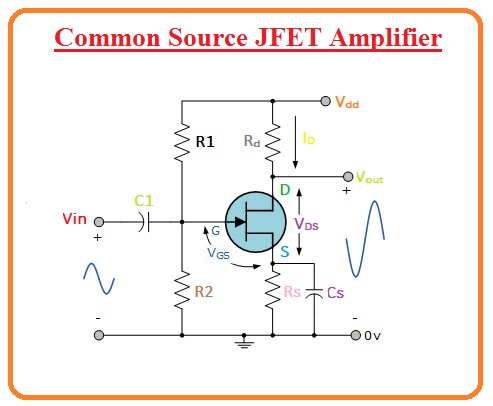
Common source jfet amplifier, common source jfet .
.

jfet circuit diagram - Wiring Diagram and Schematics

Jfet Circuit Diagram » Wiring Draw And Schematic

The basic circuit of the source-coupled JFET oscillator. | Download

jfet circuit diagram - Circuit Diagram

2N5457 N-channel JFET : Datasheet, Working & Its Applications

2N5457 N-Channel JFET Pinout, Examples, Features and Datasheet